

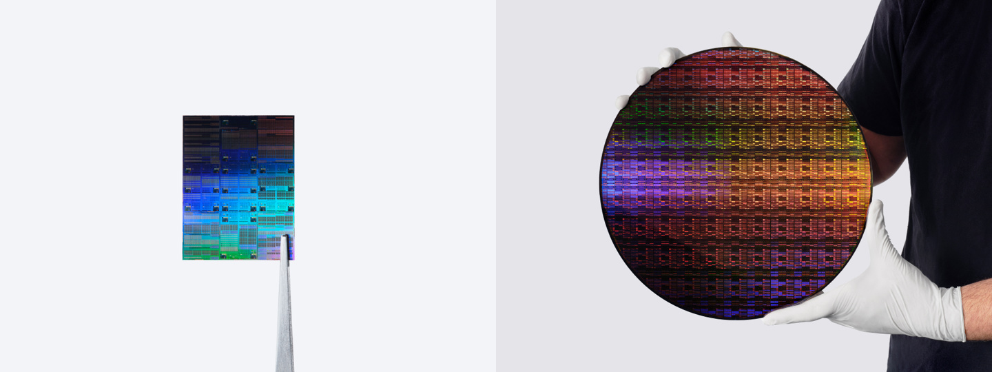
IBM and Siemens Join Forces to Advance Nanostack Chips
IBM and Siemens have announced a new research collaboration. The partnership aims to advance the IBM nanostack architecture, a transistor design IBM unveiled earlier this year.
What the Partnership Brings
According to IBM’s official press release, the deal pairs two kinds of expertise. IBM leads in semiconductor device innovation. Siemens brings deep skill in electronic design automation (EDA), process simulation, lithography optimization, and advanced manufacturing software. Together, they hope to speed up nanostack development.
The two companies will build advanced virtual models of the nanostack. Engineers can then model performance before any chip is made. In addition, they can refine designs and solve manufacturing problems early.
How the Nanostack Design Works
IBM first revealed the nanostack architecture in June. It called the design the first known three-dimensional nanosheet design in the industry. Today’s approach lays transistors flat on a two-dimensional plane and keeps shrinking the spacing. Nanostack takes a different path. It stacks transistors vertically and offsets them, so more transistors fit in the same area.
At the current 7 angstrom (0.7 nanometer) node, the design can hold nearly 100 billion transistors in an area the size of a fingernail. That density is roughly double that of IBM’s 2nm test chip from 2021. The design also allows a different material mix in each stacked layer. As a result, engineers can tune the performance and power use of every transistor on its own.
Performance and Efficiency Gains
IBM’s earlier results compare nanostack with the 2nm node. At the same power, it can deliver up to 50% more performance. At the same performance, it can cut power use by up to 70%.
At the VLSI 2026 symposium, IBM also reported a 40% scaling improvement for SRAM, or static random-access memory. This matters for AI workloads, which depend on high-bandwidth memory.
What the Executives Said
Jay Gambetta, IBM Research director, spoke at the announcement. “We are not just making transistors smaller; we are reinventing how chips are built to deliver significantly higher performance and energy efficiency,” he said.
Huiming Bu, IBM’s vice president of silicon technology research and development, offered a broader view. He described nanostack as a scalable transistor platform. It moves device scaling from two dimensions to three. In his words, it represents a new paradigm for the industry and the logic scaling path needed to support AI and other emerging technologies over the next decade.
Ankur Gupta, Siemens executive vice president of its EDA IC portfolio, stressed teamwork. He said that pushing semiconductor scaling into the angstrom era requires tight co-optimization. That effort must span device physics, EDA design and manufacturing software, and fabrication.
Bridging the Lab-to-Factory Gap
IBM has said the first products based on this technology will need about five years. Partners must then bring them into production. The new Siemens collaboration is designed to cross that gap between the lab and the factory.