

Samsung Develops New zNAND Flash for AI Workloads
Samsung Electronics is developing new NAND flash products optimized for artificial intelligence workloads. A recent report from ZDNET Korea reveals exciting details about this hardware. Specifically, the company is adding zNAND-T and zNAND-I alongside the previously announced zNAND-O.
Exploring the zNAND-T Throughput Architecture
The “T” in zNAND-T stands for “Throughput”. This design closely resembles the HBF concept introduced by SanDisk and SK Hynix. Consequently, it optimizes read and write bandwidth performance specifically for data center AI semiconductors. Furthermore, the technology utilizes TSV methodology to stack NAND dies effectively.
Understanding zNAND-I and Random Performance
Meanwhile, the “I” in zNAND-I represents IOPS. This designation symbolizes impressive random performance capabilities. Therefore, it emphasizes superior responsiveness during frequent read and write operations involving small data volumes. For instance, KV Cache offloading perfectly fits this demanding scenario.
Structural Insights and Customization Trends
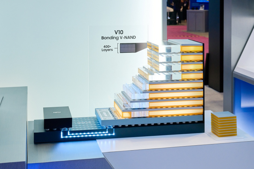
A structural diagram of zNAND-O illustrates the foundational architecture. These three zNAND variants each possess unique strengths tailored for distinct application workloads. Ultimately, they signify that NAND flash technology is rapidly transitioning from general-purpose products to highly customized AI solutions.