
Microsoft Unveils Maia 300 AI Chip
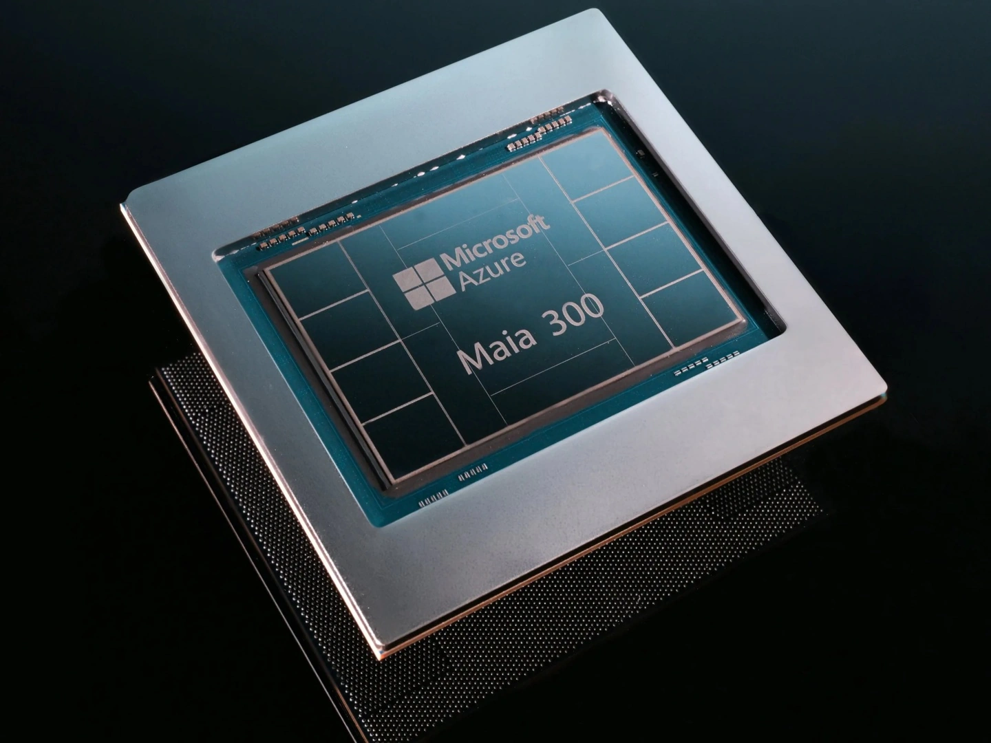
Microsoft officially released the Maia 300 AI chip today. This incredible product features 288GB of HBM4 memory. Furthermore, it delivers an astonishing memory bandwidth of 18TB/s. Consequently, its FP4 computing power reaches a massive 13.8 PFLOPS. Engineers built this silicon using the advanced TSMC N2P manufacturing process. Microsoft plans to deploy this powerful hardware in 2027.
Advanced Chiplet Architecture
The Maia 300 incorporates a sophisticated multi-chiplet design. Specifically, the primary calculation unit utilizes the cutting-edge TSMC N2P 2-nanometer process. Moreover, designers seamlessly integrated independent memory chiplets alongside dedicated I/O chiplets. Ultimately, this structural innovation maximizes overall processing efficiency.
Unmatched Compute and Power
The FP4 compute performance peaks at a remarkable 13.8 PFLOPS. Meanwhile, the FP8 compute capacity reaches 6.9 PFLOPS. Therefore, it handles highly demanding artificial intelligence operations flawlessly. The rated SoC power consumption stands at 950W. This figure is significantly higher than the 750W rating of the older Maia 200.
Exceptional Memory Specifications
Additionally, this flagship product includes eight clusters of modern HBM4 memory. The total capacity reaches a massive 288GB. Consequently, the 18TB/s bandwidth flawlessly supports memory-intensive AI inference tasks. These specifications ensure incredibly smooth data delivery during heavy workloads.
Massive Scalability and Networking
The bidirectional scale-out interconnect bandwidth achieves a blazing 3.2TB/s. Furthermore, the chip utilizes an Ethernet-based, two-tier network architecture. A single server rack can comfortably accommodate 96 Maia 300 chips. Ultimately, network engineers can build massive clusters containing up to 12,000 accelerators.